The Big Taboo in PCB Layout: A Small Mistake, a Huge Loss!
In the realm of meticulous circuit design, even the slightest error can lead to immeasurable consequences. Therefore, engineers must conduct comprehensive and meticulous checks and audits at every stage after completing the design.
Last week, a colleague finished drawing a board and sent it for sampling. However, during the wave soldering process of this circuit board, it was found that a 4-pin header component couldn't be inserted. According to feedback from the SMT assembly factory, it was because the SOIC-8 power chip overlapped with it on the back, preventing it from being inserted properly.
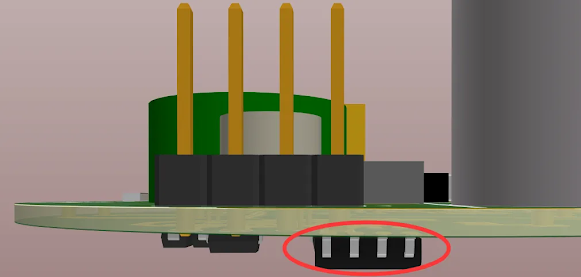
The colleague designed a compact PCB with extremely strict space constraints. Despite successfully integrating multiple complex functional modules within limited space, he inadvertently overlooked the positioning of components on the PCB's backside during the layout design process, thereby affecting the power connection and normal operation of the entire system.
However, he eventually came up with a solution: he first trimmed the obstructing header pins slightly shorter so they could be inserted, then removed the power chip, hand-soldered the trimmed header pins, and finally re-soldered the power chip. Although this process was cumbersome, it saved the hassle of redoing the board.
This example precisely underscores the importance of precision and thoroughness in circuit design. While engineers pursue technical breakthroughs and innovation, they must always maintain precise control over every detail, ensuring that any potential issues can be anticipated and addressed during the design phase.
Only in this way can the final product perfectly leverage design efficiency, meet the requirements of practical application scenarios, and avoid the incalculable losses that may result from a momentary oversight.
Afterwards, I introduced my colleague to the inspection tool: Huachuang DFM software. Because it not only checks for design issues but also helps to avoid potential production problems, verifying whether the PCB design is suitable for manufacturing and assembly.
At first, he was skeptical, so I imported the design files into the Huachuang DFM software and conducted an SMT analysis in front of him. The software immediately flagged an "interference" issue with the through-hole pins in the "through-hole pins" check item.
Well, this directly saved half of the inspection effort and time. He said it was simply a tool for being lazy.

This reminds me of another incident, from a conversation with an experienced technician who repairs circuit boards. He mentioned that once while fixing a board, he found a small resistor burnt out, but it was partially obstructed by a digital display. To repair it, he would have to remove the digital display, but this process carried significant risk, as it could damage the display.
Upon hearing this, I immediately realized that it was likely due to the designer placing the resistor under the digital display to save space and simplify wiring, without considering the issue of future maintenance. The technician said there was no choice but to cautiously remove the digital display.
Therefore, when we're designing, we must consider all aspects and not just focus on convenience, as it could create more trouble for maintenance in the future, leading to even greater losses. When it comes to layout design, attention to detail is crucial, with no room for negligence.

Moreover, to validate this, I deliberately created a case and imported it into the Huachuang DFM software for SMT assembly analysis. Sure enough, the software flagged a red alert under the "Component Spacing" check item, indicating not only insufficient spacing but also marking the specific locations.

Huachuang DFM software is the first free PCB manufacturability and assembly analysis software in China, with a component library of over 5 million parts, enabling easy and efficient assembly analysis. Its PCB bare board analysis function covers 28 major items and 52+ detailed inspection rules, while the PCBA assembly analysis function covers 12 major items and 600+ detailed inspection rules.
It essentially covers all possible manufacturability issues, helping design engineers detect manufacturability problems before production and catering to various scenarios required by engineers, thereby minimizing the number of product development iterations and reducing costs.


Comments
Post a Comment